|
|
|
|
中文版 | News | Archives | Reviews | Forum | $ Deals | Links | History | Contact | Privacy |
|
| ||||
|
ASUS A7N8X nForce2
Mainboard Gallery (3)
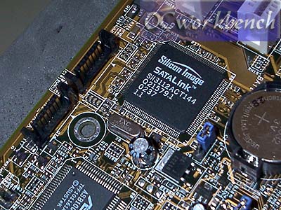
The SATA connector supported by the SiliconImage SATALINK chipset Sil31122
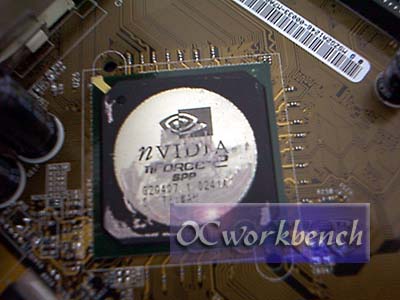
nVIDIA nForce2 SPP chipset is the North bridge controller chipset. It supports a 64/128bit DDR memory controller and up to 3GB of DDR 400/333/266/200 memory. During our test, we are able to run Dual DDR400 in a Dual memory setup.
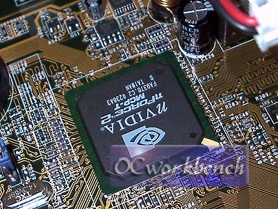
The MCP-T chipset is the south bridge operates at 800MB/sec to communicate with the NB for max. bandwith required for PCI/USB, and fast ethernet devices. The chipset has an integrated APU for Dolby digital encoding. It supports ATA133 disk. It also supports 2 1394 ports (optional), 6 USB ports, 2 LAN ports (optional).
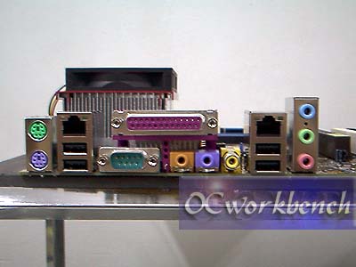
The connectors on the rear of the mainboard.
Dual LAN ports one supported by 3COM and the other by nVIDIA. The Orange port is
the Cntrl / LFE connector, purple port is Surround L/R connector, yellow port is
the S/PDIF out connector. Line in (blue), Line out (green), Microphone connector
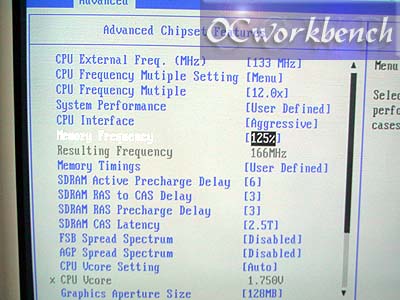
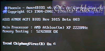
(pink). The BIOS Advanced chipset features allows you to tweak many options to ensure maximum compatibility or performance. In our 1005.003 BIOS, we have a number of default settings like Optimal (which is SPD), advanced and user define. We user define all our test settings for RAM to run at DDR333 and DDR400. We tested it in 3 configurations, 1 x DDR333 (512M), 2 x DDR333 (256M) and 2 x DDR400 (256M) all at CAS 2, active precharge = 5, RAS to CAS = 2, RAS Precharge Delay = 2. FSB is selectable from 100 ~ 200 at 1mhz steppings (after 133, from 100 - 132, some are at 2mhz steppings). There are also various FSB that are above 200Mhz if you were to use optimal timings. The Memory Frequency can be selected from various percentages. For example, setting is to 125% will run it at 166 Mhz (DDR333), 150% will be 200Mhz (DDR400)
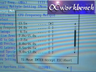
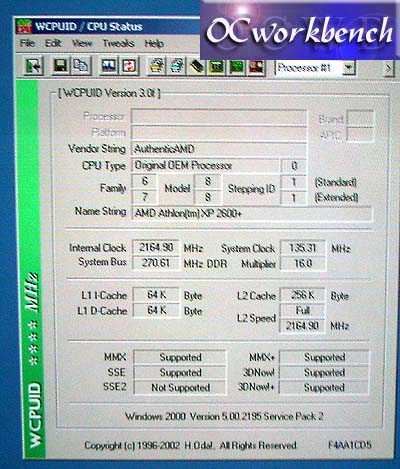
CPU Multiplier is selectable to 17x. BIOS settings We are able to overclock the CPU to run at 2600+ by changing the multiplier of 8x/16x using a Tbred 2400+
Overclocked to 16x (2600+) by changing the multiplier of a TB 2400+
Screen shot of AXP 2400+ o/c to POST at 16.5x
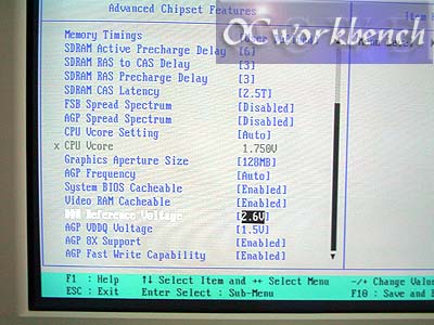
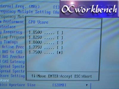
CPU Vcore can be set to a maximum of 1.850v
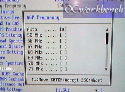
Something that is uncommon on AMD boards. This is probably the first board that implements a FIX AGP selection. You can fix the AGP to run at 66mhz no matter what is your FSB. A maximum of 100Mhz can be chosen.
|
|
(C) Copyright 1998-2009 OCWorkbench.com
|