|
|
|
|
中文版 | News | Archives | Reviews | Forum | $ Deals | Links | History | Contact | Privacy |
|
| ||||
ASrock P4 Combo Intel 848P Socket 478/775 Mainboard
Gallery 2/4
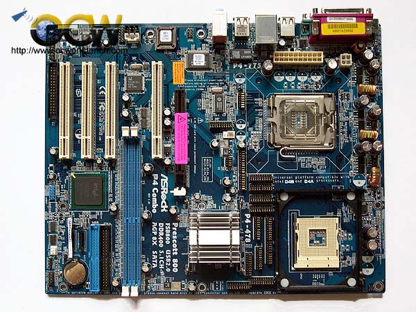
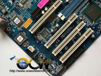
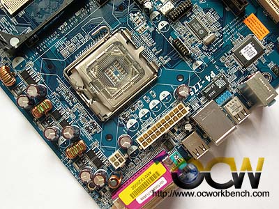
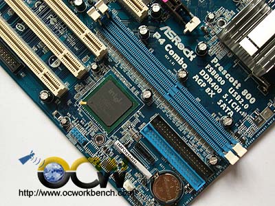
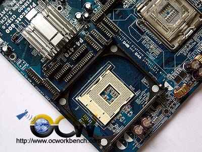
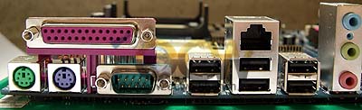
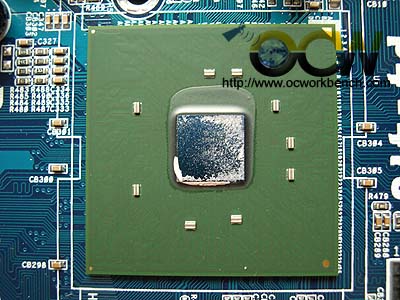
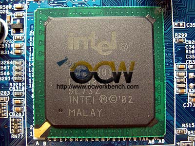
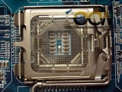
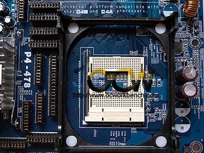
Gallery The north bridge which is the i848P is located near the Socket 478 socket. It uses a passive heatsink which gets hot after benchmarks are run. I replaced the thermal pad with thermal paste to help dissipate the heat. On the left of the chipset 848P are two DIMM slots, 2 IDE and 2 SATA ports. ICH5 south bridge is located right next to the SATA ports. On the right you will see many blocks of jumpers. The board comes default jumper setting for P4 S478. In my case, after testing the P4 S478, I need to change the positions from 2-3 to 1-2 for the all the jumper blocks. It is quite tedious if you were to count how many of them are there on the mainboard. Next to all the jumpers is the Socket 478 socket. On the top corner of the board, there is the floppy connector, 3 PCI and 1 AGP 8x Slot/PCI Slot which shares a common slot on PC casing. Next to it is the Socket 775 for the LGA775 Prescott. On the right most is the 3 phase power design for stability of the board. At the back panel, there are 6 ready to be used USB ports. 2 more can be added to make up 8 USB 2.0 ports.
Next >>> |
|
(C) Copyright 1998-2009 OCWorkbench.com
|