中文版 | News | Archives | Reviews | Forum | $ DealsLinks | History | Contact | Privacy

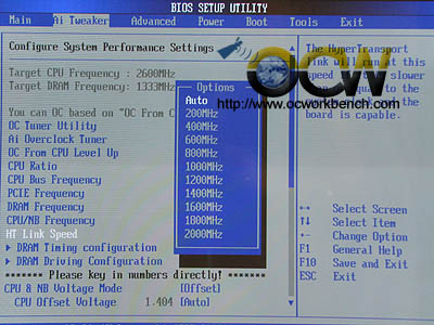
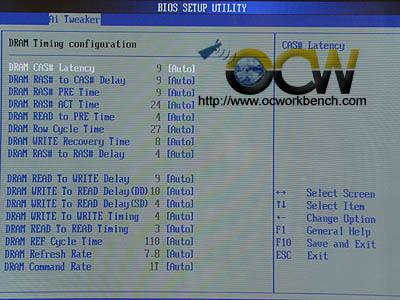
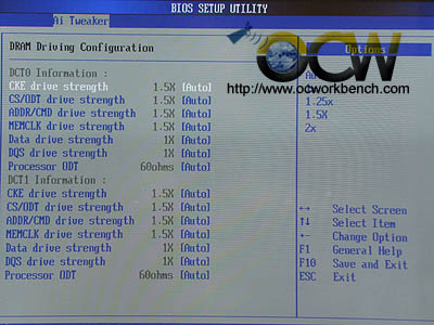
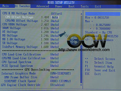
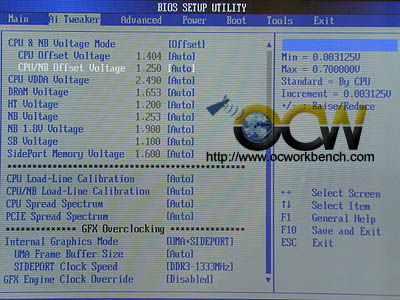
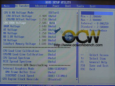
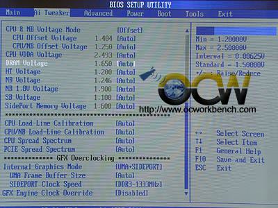
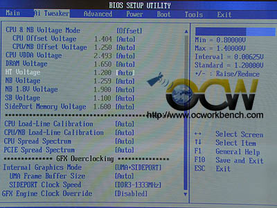
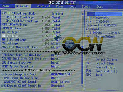
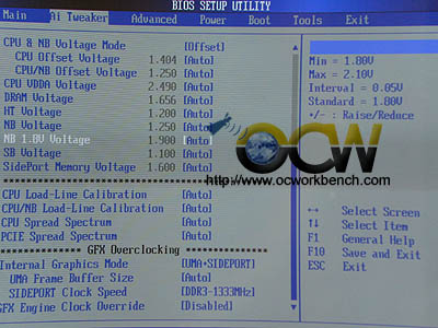
BIOS Screen shot 2 of ASUS M4A89GTD Pro/USB3 AMD 890GX+SB850 mainboard
Bluetooth 27 Feb 2010

BIOS 2

HT link speed can be lowered to achieve higher CPU CLK

The DRAM timings detected. It can be adjusted to speed up your system.

DRAM Driving configuration for the experts to fine tune it for various rams In this page, it is where all the voltage levels can be set for the various NB, SB, HT, SP etc.
CPU/NB offset voltage from 0.003125 to 0.7v CPU Vdda from 2.290 to 2.90v
DRAM voltage from 1.20 to 2.5v HT voltage from 0.8v to 1.40v
NB voltage from 0.8v to 2.0v NB 1.8v voltage from 1.80v to 2.10v


Discuss in Forum

g1,g2,g2a,g3,g4,g5,g6,b1,b2,b3,b4,b5,b6,b7,b8,b9,b10

Next >>>

(C) Copyright 1998-2010 OCWorkbench.com